Specifications︰
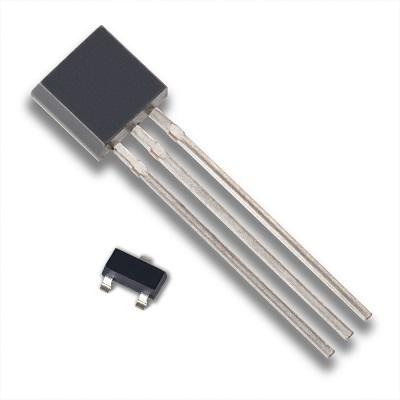
LSK189 TO-92 3L
LSK189 SOT-23 3L
Advantages︰
A low noise JFET such as an LSK189 is configured as a
source follower, with a source biasing resistor R3. In
terms of input capacitance at the gate of J1 with an
LSK189, it is about 3 pF from the gate to the drain,
which is much less than the 18 pF of Cin(-).
Capacitance between the gate and ground due to the
gate to source capacitance approaches zero. This is
because the source follower configuration provides
substantially the same AC voltage at the gate and at
the source, which substantially cancels out the
capacitance between the gate and the source. The
source follower also greatly reduces the capacitance
seen at the gate to ground even when the source is
driving signal into a capacitive load, Cin(-), the
capacitance at the (-) input terminal of the op amp
U1A.
It should be noted that the source follower circuit
may add some phase shift to the overall amplifier
circuit. To ensure phase margin and no oscillations, a
resistive divider R1 and R2 is used. With the values
given at 3900Ω for R1 and R2, the equivalent
feedback resistance is [1 + (R2/R1)] x RF = 2 x 1MΩ =
2MΩ, the same resistance value shown in Figure 8
for RF.
If the (+) input of the op amp in Figure 9 is grounded,
such that Voffset = 0 volts, Vout will most likely have
a DC offset. To “zero” Vout when there is no signal
from the photodiode, a clean DC voltage, Voffset may
be applied to the (+) input of U1.
Op amp U1A = AD797 has an equivalent input noise
voltage of 0.9 nV/ 𝐻�𝑧� and J1 =LSK189 with an
equivalent input noise voltage of 1.8 nV/ 𝐻�𝑧�, the
total equivalent input noise voltage is about 2.0
nV/ 𝐻�𝑧�. This is lower than a very low noise JFET op
amp such as an AD743 that has 3.2 nV/ 𝐻�𝑧�. Note
that bipolar input stage op amps AD797 with 0.9
nV/ 𝐻�𝑧� has lower equivalent input noise voltage
than 2.0 nV/ 𝐻�𝑧�, but the AD797’s input noise
current is too high and are not suitable for amplifier
circuits with large value feedback resistors (RF) in the
MΩ such as the circuit shown in Figure 8.
Note that J1 may be substituted with an LSK170
(0.9nV/ 𝐻�𝑧� ) if a slight increase in capacitance from
the gate to ground is acceptable. This FET has about
half the equivalent input noise of the LSK189.

